Overview
The question and its context.
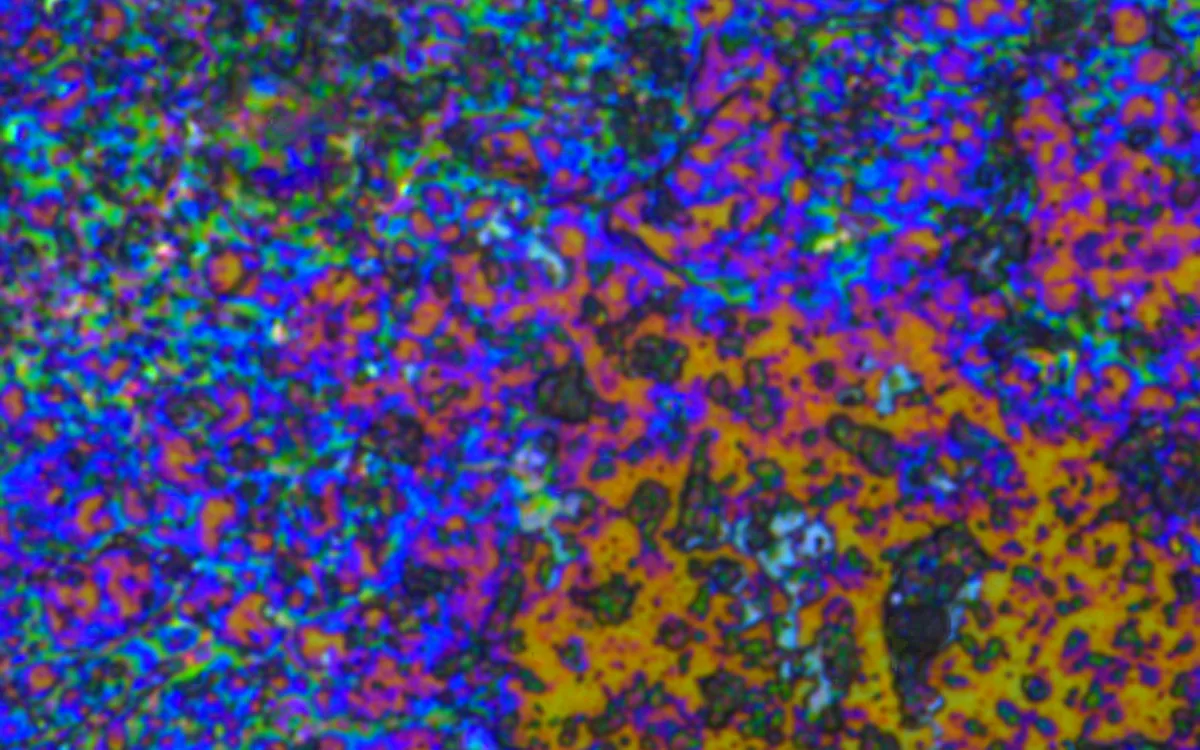
Two-dimensional materials and semiconductors provide a platform for investigating nanoscale surfaces and interfaces. This project presents a microscopy view of MoTe₂, focusing on the surface structure visible in the supplied image.
Approach
Methods, decisions, and collaboration.
Colour-enhanced microscopy highlights variations in surface morphology across the material. The image supports close inspection of texture, contrast, and structural features throughout the sample.
Outcome
Outputs and evidence of value.
The microscopy image provides a visual record of the MoTe₂ surface for further structural interpretation and comparison within 2D materials and semiconductor research.